Serial Peripheral Interface Bus
The Serial Peripheral Interface (SPI) bus is a synchronous serial communication interface specification used for short distance communication, primarily in embedded systems. The interface was developed by Motorola and has become a de facto standard. Typical applications include Secure Digital cards and liquid crystal displays.
SPI devices communicate in full duplex mode using a master-slave architecture with a single master. The master device originates the frame for reading and writing. Multiple slave devices are supported through selection with individual slave select (SS) lines.
Sometimes SPI is called a four-wire serial bus, contrasting with three-, two-, and one-wire serial buses. The SPI may be accurately described as a synchronous serial interface,[1] but it is different from the Synchronous Serial Interface (SSI) protocol, which is also a four-wire synchronous serial communication protocol, but employs differential signaling and provides only a single simplex communication channel.

Single Master Multi Slave

Interface ->
SCLK -> Clock from master to slave
MOSI -> Master Out Slave In
MISO -> Master In Slave Out
SS -> Slave Select
Data Transmission
To initiate a transaction, Master first assert slave select line to select the slave.Typical data transmission size is 8-bit , but it can be specific to it's usage and bit size can be anything (Application specific , Master and Slave will have to re-design to support odd size of transaction).
During each SPI clock cycle, a full duplex data transmission occurs. The master sends a bit on the MOSI line and the slave reads it, while the slave sends a bit on the MISO line and the master reads it. This sequence is maintained even when only one-directional data transfer is intended.
Transmissions normally involve two shift registers of some given word size, such as eight bits, one in the master and one in the slave; they are connected in a virtual ring topology. Data is usually shifted out with the most-significant bit first, while shifting a new least-significant bit into the same register. At the same time, Data from the counterpart is shifted into the least-significant bit register. After the register bits have been shifted out and in, the master and slave have exchanged register values. If more data needs to be exchanged, the shift registers are reloaded and the process repeats. Transmission may continue for any number of clock cycles. When complete, the master stops toggling the clock signal, and typically deselects the slave.
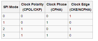
SPI MODE
- For CPHA=0, data are captured on the clock's rising edge (low→high transition) and data is output on a falling edge (high→low clock transition).
- For CPHA=1, data are captured on the clock's falling edge and data is output on a rising edge.
- For CPHA=0, data are captured on clock's falling edge and data is output on a rising edge.
- For CPHA=1, data are captured on clock's rising edge and data is output on a falling edge.
A Summary table is given below.
Advantages
- Full duplex communication in the default version of this protocol.
- Push-pull drivers (as opposed to open drain) provide good signal integrity and high speed.
- Higher throughput than I²C or SMBus.
- Complete protocol flexibility for the bits transferred
- Not limited to 8-bit words
- Arbitrary choice of message size, content, and purpose
- Extremely simple hardware interfacing
- Typically lower power requirements than I²C or SMBus due to less circuitry (including pull up resistors)
- No arbitration or associated failure modes
- Slaves use the master's clock, and do not need precision oscillators
- Slaves do not need a unique address — unlike I²C or GPIB or SCSI
- Transceivers are not needed
- Uses only four pins on IC packages, and wires in board layouts or connectors, much fewer than parallel interfaces
- At most one unique bus signal per device (chip select),all others are shared Signals are unidirectional allowing for easy Galvanic isolation.
- Not limited to any maximum clock speed, enabling potentially high speed
Disadvantages
- Requires more pins on IC packages than I²C, even in the three-wire variant
- No in-band addressing; out-of-band chip select signals are required on shared buses
- No hardware flow control by the slave (but the master can delay the next clock edge to slow the transfer rate)
- No hardware slave acknowledgment (the master could be transmitting to nowhere and not know it)
- No error-checking protocol is defined
- Without a formal standard, validating conformance is not possible
- Only handles short distances compared to RS-232, RS-485, or CAN-bus
- Many existing variations, making it difficult to find development tools like host adapters that support those variations
- SPI does not support hot swapping (dynamically adding nodes)
- Interrupts must either be implemented with out-of-band signals or be faked by using periodic polling similarly to USB 1.1 and 2.0
- Typically supports only one master device (depends on device's hardware implementation)
No comments:
Post a Comment